")
The Semiconductor Cleanroom

In today’s fast-paced technological landscape, we often take for granted the intricate marvels that power our devices – from smartphones to laptops and beyond. Behind the scenes, a symphony of advanced engineering and scientific precision is at play, and at the heart of it all lies the semiconductor industry. This industry is the cornerstone of modern innovation, propelling us into a future of endless possibilities. However, the journey from concept to consumer-ready technology is far from simple; it’s a meticulous dance that takes place in a controlled environment known as the cleanroom.
Understanding the Semiconductor Industry
Before diving into the significance of cleanrooms, let’s understand the basics of the semiconductor industry. Semiconductors are materials with properties that are neither fully conductive nor fully insulative, making them ideal for controlling electrical current. These materials serve as the building blocks for electronic devices, ranging from microprocessors to memory chips. Their tiny size and incredible processing power are the result of intricate manufacturing processes performed in cleanrooms.
The Crucial Role of Cleanrooms
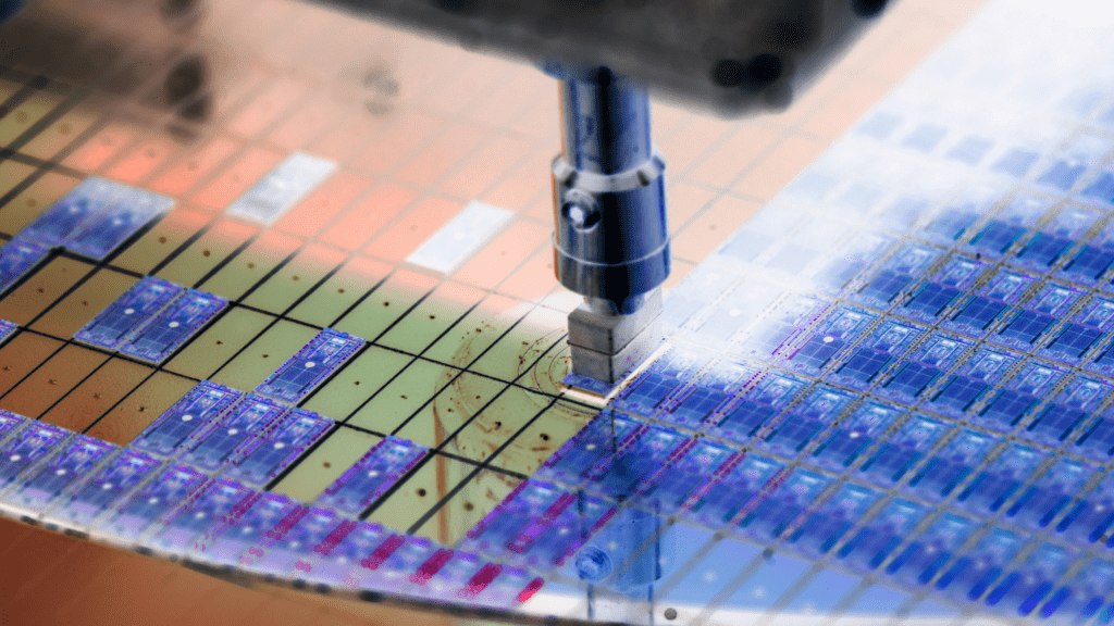
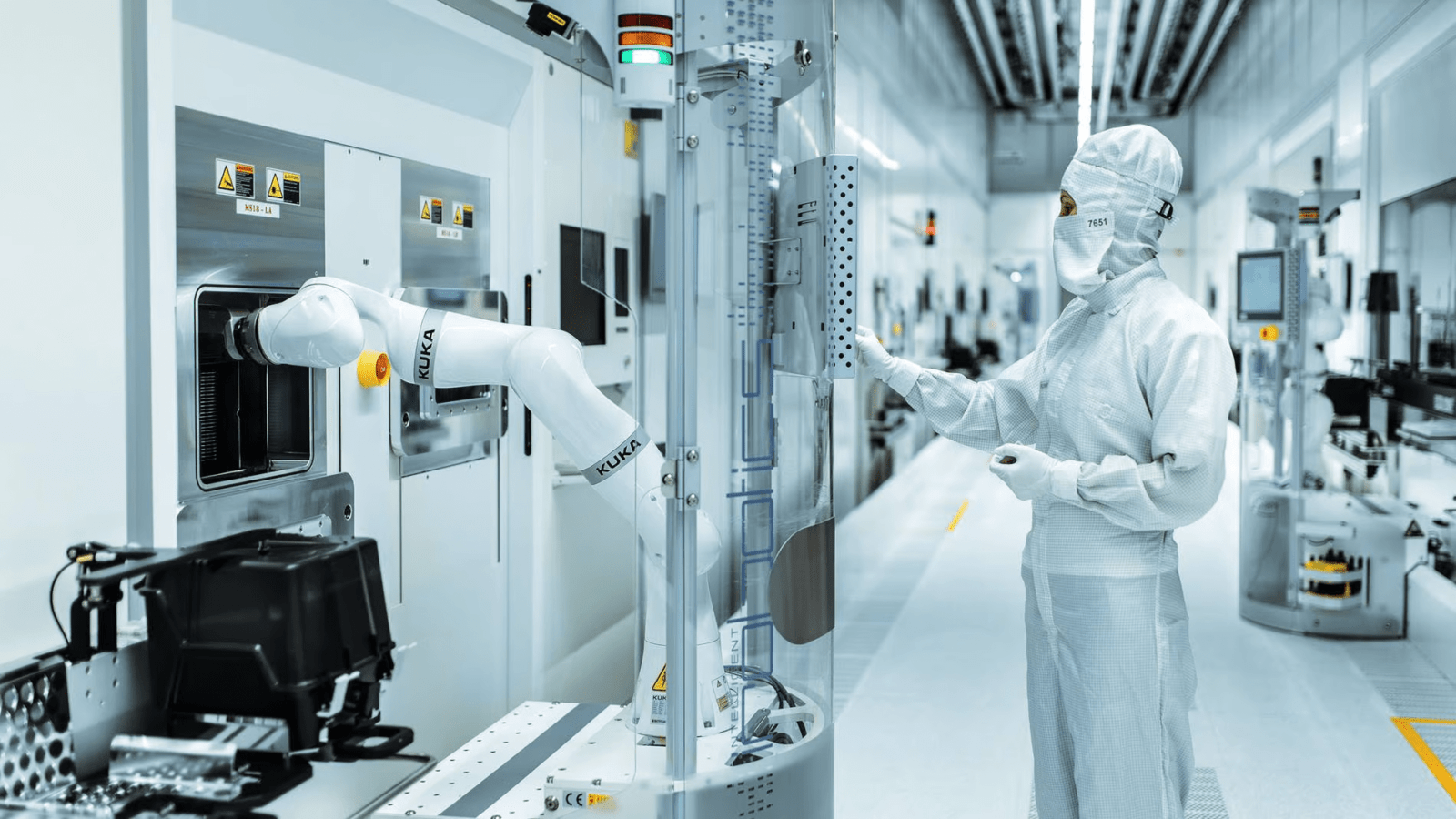
Cleanrooms are specialized environments designed to maintain extremely low levels of airborne particles, such as dust, microbes, and chemical vapors. These particles can significantly impact the performance and reliability of semiconductor devices. A single speck of dust, invisible to the naked eye, can disrupt the delicate circuits etched onto a semiconductor wafer.
The semiconductor manufacturing process involves multiple steps, including photolithography, etching, doping, and deposition. Each of these processes requires a pristine environment to ensure the accuracy and consistency of the resulting components. Cleanrooms provide a controlled space where temperature, humidity, and air cleanliness are maintained at stringent levels, minimizing the risk of contamination during these delicate operations.
Design Considerations
The design of a semiconductor cleanroom involves meticulous planning to minimize any external contaminants that could compromise the quality of the final products. Some key design considerations include:
- Air Quality and Filtration: High-efficiency particulate air (HEPA) filters are used to remove particles from the air, ensuring a controlled environment with minimal dust or foreign particles.
- Temperature and Humidity Control: Maintaining a consistent temperature and humidity level is crucial to prevent variations in the manufacturing process, which can affect the electrical properties of semiconductor materials.
- Airflow Control: The direction and velocity of air movement are strategically designed to prevent the accumulation of particles and ensure uniform conditions throughout the cleanroom.
- Cleanroom Layout: The layout is carefully planned to separate different manufacturing processes and minimize the risk of cross-contamination.
- Material Selection: Materials used in the cleanroom, such as flooring, wall coverings, and furniture, are chosen to minimize particle generation and facilitate easy cleaning.
Cleanroom Classifications
The International Organization for Standardization (ISO) has established a widely accepted classification system for cleanrooms, denoted as ISO 14644. This system defines the allowable particle counts per cubic meter of air at specified particle sizes. The ISO cleanroom classification numbers range from ISO 1 (the cleanest) to ISO 9 (the least clean), with each class representing a specific threshold for airborne particle concentration.
Semiconductor cleanrooms often need to adhere to ISO Class 1 to ISO Class 6 classifications due to the delicate nature of chip manufacturing. These classifications ensure an environment where even the smallest particles are minimized, safeguarding the integrity and reliability of the produced semiconductor devices.
Battle Against Contaminations
Contaminations within a semiconductor cleanroom can arise from various sources, such as personnel, equipment, raw materials, or the surrounding environment. Even a single dust particle can disrupt the functionality of an intricate semiconductor device. To combat this, cleanroom operators employ a variety of strategies:
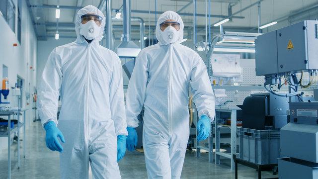
- Personnel Protocol: Strict gowning procedures, including specialized cleanroom attire, are enforced to prevent human contaminants from entering the controlled environment.
- Equipment Maintenance: All tools and equipment used within the cleanroom are regularly cleaned and maintained to prevent particle generation.
- Material Handling: Raw materials and components entering the cleanroom are carefully inspected and cleaned to prevent the introduction of contaminants.
- Cleanroom Behavior: Cleanroom personnel are trained to follow specific protocols, including movement patterns and working practices, to minimize the dispersion of particles.
The semiconductor industry’s journey from raw materials to intricate microchips is a testament to human ingenuity and scientific advancement. Cleanrooms, often overlooked by the general public, are the unsung heroes of this progress. These controlled environments ensure that the technologies of tomorrow are not compromised by the invisible particles that surround us. As we marvel at our ever-smaller, more powerful devices, let’s remember that it all starts with the meticulous orchestration of a cleanroom – where groundbreaking ideas come to life, one particle-free space at a time.
ARE YOU LOOKING FORWARD TO BUILD A SEMICONDUCTOR CLEANROOM? LET’S CONNECT.
If your organization is on the brink of a semiconductor cleanroom endeavor, look no further than ACH – A Cleanroom Hub. Our expertise lies in designing, constructing, and installing cutting-edge cleanrooms that align seamlessly with your unique requisites. With a track record of using tried-and-true design approaches and using static dissipative materials, we guarantee that your projects and workforce will remain safe and thriving. Don’t delay – reach out today, and let’s transform your vision into a meticulously designed reality!
Request for a free quote, or contact our team for further information.
GET IN TOUCH
Complete the form below to get in touch with our team.