")
")
The World of the Semiconductor Cleanroom

In the current era, imagining human life without electronic devices is impossible. Electronic media such as televisions, cell phones, computers, smartwatches, and more are an integral part of daily life. The concept that made such amazing technology a reality is the silicon chip, or, semiconductor.
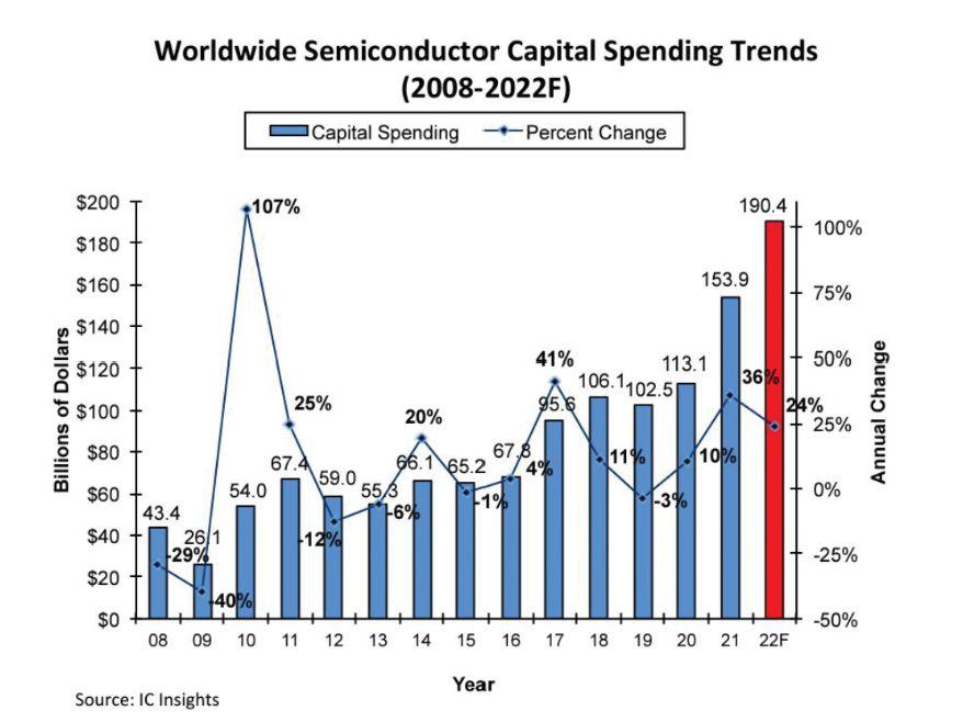
The demand for semiconductors is rising every day due to its consumption at almost every level of civilization. According to a market survey conducted by IC Insights, the total capital spending on semiconductors has increased from $43 Billion to $194 Billion since 2008, including a 36% rise in 2021, and a 24% rise in 2022.
Manufacturers now look to improve fabrication efficiency and sustainability, to develop a better production environment. To understand what standards are required for semiconductor manufacturing, one must first understand what a semiconductor is.
What is a Semiconductor?
Semiconductors are glassy or crystalline solids with specific electrical characteristics. Semiconductors create a unique conductivity when placed between conductors – usually metals – and nonconductors or insulators. They are typically made of elements such as silicon or germanium and are referred to as microchips or integrated circles. Their electrical properties can be adapted to allow augmentation and energy conversion.
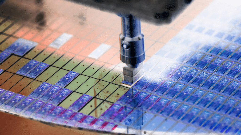
The production of semiconductors begins with the most common element on earth – silicon. Silicon is refined to achieve 100% purity before being manufactured, because it is primarily found in sand. For the silicon chip to function correctly, the silicon must be of absolute clarity, as the slightest imperfection can render the chip inoperative. Silicon is heated until it becomes molten to achieve a state of pure clarity.
The properties of molten silicon make it possible to create a chemical bond between the silicon “seed,” which is placed inside a molten state, and the chunk of solid silicon, which forms as silicon cools. The end result is a finished block which imitates the physical characteristics of the original seed matter. Later, the block is sawed into perfectly round, thin wafers and shipped to the cleanroom for further development.
Health Risks Associated with Semiconductor Manufacturing
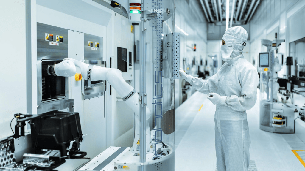
Thin wafers go through a complex of heavy chemicals and electrical charges, building up distinct layers to become functioning semiconductors. The wafers go through different types of equipment and machinery that apply every necessary chemical level. Sometimes it might take up to a year of constant chemical processing before the semiconductor is complete. Specific machines involved in processing the wafers use radioactivity, lasers, magnetic fields, highly reactive chemical exposures, and photolithography. Both people and robots operate the equipment depending on the sophistication level of a manufacturing cleanroom.
Unfortunately, as long as heavy chemicals are being used for production, there will always be a higher exposure risk to operators. Particular safety protocols and methods should be enacted to protect everyone working in a semiconductor cleanroom.
It is known that some chemicals used during production could cause health problems, especially in the female reproductive systems. Even though exact scientific data is unconfirmed and outdated, there still remains reason for concern.
Hydrofluoric acid, fluorine, tetraethylorthosilicate, and arsenic are just a few dangerous chemicals used during manufacturing. Although operators don’t handle the chemicals directly, it can be hazardous working around them if the particular requirements (such as proper air filtration) aren’t met.
Nowadays, manufacturing companies claim to disregard chemicals that were once a concern for personnel health. Even though there are very few reports on the immediate consequences of working in such facilities, not much research has been done on the long-term effects. That is why it’s especially important that all operators should exercise caution and follow the necessary protocols to protect themselves.
Risk Mitigation with Cleanroom Considerations
When a speck of dust is enough to affect the performance of a chip, controlling the environment is the only way to reduce the risk of contamination. To ensure the cleanroom environment is always controlled, it should be engineered in a certain way. It must control static, outgassing, particular matter, and other compromising conditions. Here are the most vital requirements to consider.
- The air in the cleanroom must always be maintained at the required purity levels. Most frequently, semiconductor cleanrooms require an ISO 14644 Air Cleanliness Standard. Proper airflow arrangements play a critical role in maintaining air purity.
- Vertical Laminar Flow (unidirectional) serves best in semiconductor cleanrooms. Air is blowing from the ceiling to the floor in a constant uniform stream. Once it reaches the bottom, it goes down through the holes in the flooring to be purified by HEPA filters.
- Another consideration to keep in mind is the layout of the equipment. A recommendation is for the workbenches and equipment to be placed along outer walls to avoid areas with maximum airflows. Flat surfaces and corners should be eliminated if possible so that contaminating particles are not collected on them.
- Employees must follow all methods and protocols to avoid adding contamination to the cleanroom.
Do you have a semiconductor cleanroom project in mind? Let’s talk! Contact us today!
GET IN TOUCH
Complete the form below to get in touch with our team.